The µPD861 PLL
Not a lot has been written about this versatile PLL chip. When a novice hack goes to modify the chip for frequency expansion, they often shake their head at the frequencies showing up on their freq. counter as they spin the channel selector. There's a reason for that, and we are going to find out why.
First of all let's examine the pinout of the
uPD861 PLL, mfg. by NEC:
Sub: ECG1254 (Sylvania)
| P1 | 1 | 24 | (1) |
| P2 | 2 | 23 | Vss |
| P3 | 3 | 22 | LD* |
| P4 | 4 | 21 | PD |
| P5 | 5 | 20 | AI |
| P6 | 6 | 19 | AO |
| P7 | 7 | 18 | (5) |
| P8 | 8 | 17 | (2) |
| 1/2R | 9 | 16 | (3) |
| RI | 10 | 15 | (4) |
| RO | 11 | 14 | MS** |
| Vdd | 12 | 13 | Fin |
* 1 = Locked, 0 = Unlocked
** Mode Select: 1 = 40 Channel BCD/ROM,
0 = 8-bit binary (n of 3 to 255) using pins 1-8.
(1) Inhibit. Goes HIGH in BCD/ROM mode for non-legal program.
Disconnect if not disconnected already.
(2) Reference Divider output
(3) PD in from Reference Divider
(4) Programmable Divider Output
(5) PD in form Programmable Divider
The first thing notable about this chip is that it has two modes of programming: Straight binary (with an 'n' of 3 to 255) or BCD/ROM (with the only 'n' codes available being 91-135). The 'mode' of this chip (binary/BCD) is determined by voltage (~+8VDC) present at pin 14. If +, then BCD/ROM. If pin 14 is grounded, then straight binary programming may be used. There is another gotcha here: In BCD/ROM mode 'n' is preset to 90 plus 'n', such that on channel ONE, the only programming pin on the chip that has +DC is pin one, leading you to believe that 'n' is '1' instead of '91'. Also, in BCD/ROM mode, programming is six bit, with only the first six programming pins used. The state of bits 7 and 8 in BCD mode are ignored.
The above is great, but what does that
mean? Can I modify this thing? Will it be a useful mod? Yes and Yes.
As mentioned by others, there is no cookbook method for modifying this chip
documented anywhere. If the rig is already in binary mode, then follow
binary programing modification of PLL chips that has been documented ad nauseum
elsewhere.
Here is a partial chart of which rigs are which:
| BCD/ROM
Programming AM Models: |
Binary Programming AM Models: |
?? Programming |
|
Boman CBM-6100 Colt 350 Convoy CON-400 SBE 49CB JC Penney 981-6221 JC Penney 981-6203 JC Penney 981-6237 JC Penney 981-6255 Realistic TRC440 Realistic TRC461 Realistic TRC466 Realistic TRC467 Realistic TRC468 Sears 934.3806 Sears 934.3808 Sears 934.380817 Sears 934.381107 Sears 934.381207 TRX Challenger 600 |
Panasonic RJ-3250 Panasonic RJ3450 Panasonic RJ3600 Panasonic RJ3660 Realistic TRC424 Realistic TRC431 Realsitic TRC456 Superscope Aircommand CB140 Superscope Aircommand CB340 Superscope Aircommand CB640 |
CDE Mark 26 Contact PSC301 Pearce-Simpson Super Bengal Mark II Wagner 510 |
We're going to talk about modifying the frequency
coverage of a Rig with the PLL in BCD/ROM mode. 'n' codes will be 91-135
for the US rigs.
The first step is to disconnect pin 24 of the PLL from the circuit board. Do
this by cutting the foil trace that leads to the pin or desolder the pin or cut
the pin. Careful. This disables the inhibit function of this chip
which shuts down the VCO should an illegal program be present.
The second step is to purchase a SPDT (or use a convenient switch inside the
radio such as a Tone or NB switch) to control whether the PLL is operating in
BCD/ROM or Binary mode. Do this by isolating pin 14 (the 'mode select'
pin) on the PLL. Connect this pin via a wire to the middle leg of your
SPDT switch. Connect the bottom leg to an 5-8v power source such as pin 12
of the PLL. Connect the top leg of your SPDT switch to circuit board
ground, such as pin 23 of the PLL. Should look something like this:
(SW1)
S    	|_____GND
	|
P	|_____Pin 14 of uPD861
	|
D	|_____+DC
	|
T	|
The above switch will control whether the rig is in BCD/ROM ('Normal' 40 Channel) mode or Binary Mode. (High and Low Frequencies!!!) There's more to do yet, but you can test your rig to see if everything operates as normal with the switch in the down position. At this point, putting the switch in the 'up' position will most likely change the chip programming so dramatically that the VCO will shut down. That is perfectly normal at this point.
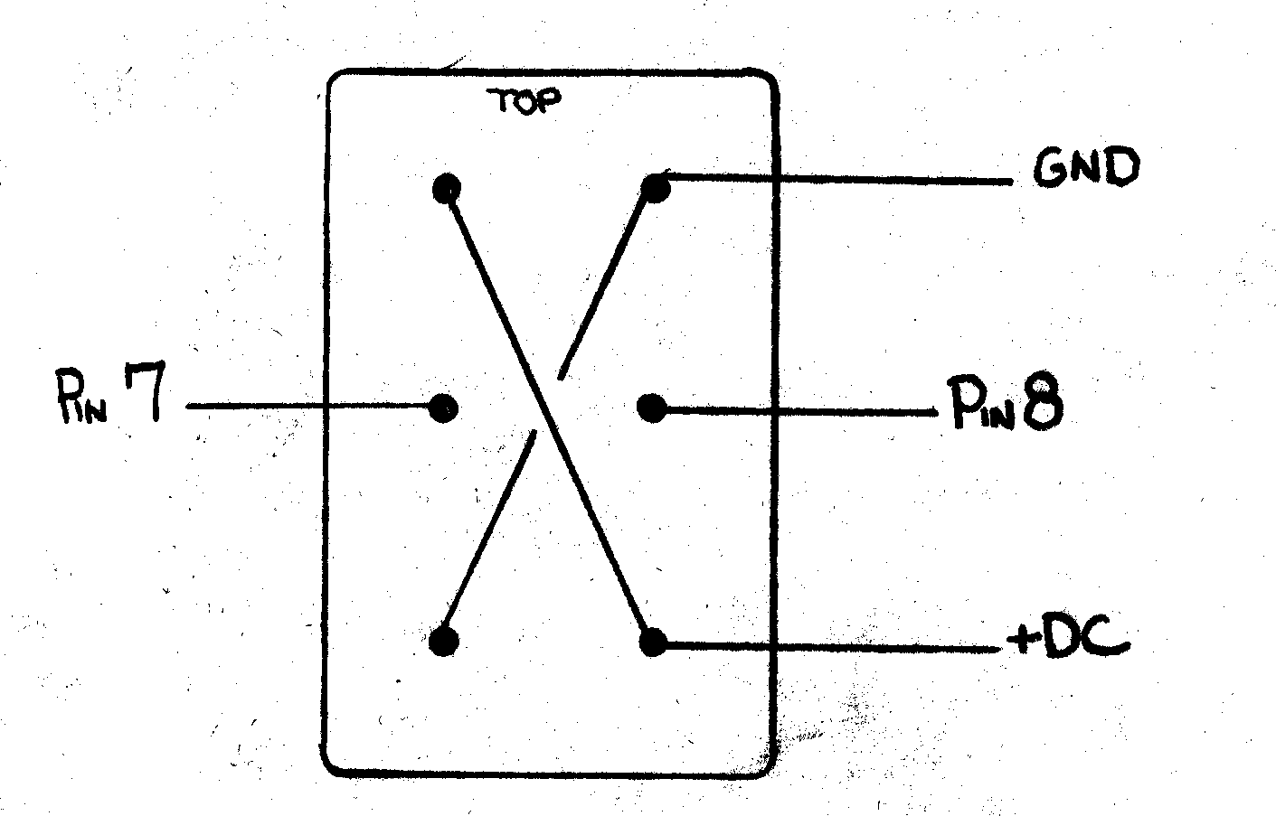
The third step is to control the states of PLL
pins 7 and 8 while the rig is in Binary Programming Mode (1st switch in 'up'
position). Doing this will allow us to go below and well above the normal
FCC channels, and we'll see why a little later. You'll need a DPDT
switch. If there is a convenient switch of this type in the radio, then by
all means use it. Otherwise, obtain a switch and mount it in a secure
location in the radio. Isolate pins 7 and 8 of the uPD861 PLL by cutting
their foil traces on the circuit board near the PLL pins. Also make sure that
pins 7 and 8 are isolated FROM EACH OTHER, as they are often soldered to ground
on the circuit board by a common 'pad' of solder. Hook up your DPDT
switch as follows:
(SW2)
After you have this switch hooked up, it will be time to test the 'new' frequencies of the rig. As I mentioned earlier, this is where some people get flummoxed when they observe the new frequencies on a freq. counter. The frequencies don't follow the normal 450 KHz 'pattern' of the FCC legal 40 channels. The explanation of this lies in the 'n' code the PLL is receiving. When the first switch is in the down, or 'normal' position, everything works like a stock radio. But when the Binary Mode is selected and the second switch is in the 'upper' or 'high' position, a band of frequencies is produced, but the progression of the frequencies doesn't make sense (at first). The explanation for all of this can be obtained by the 'truth chart' I have prepared below. Teamed with this chart and the knowledge that you are using a BCD channel selector and that you have forced the PLL into binary mode will shed some light on the frequency progression.
Truth and Frequency Chart for the 'new and improved' uPD861c:
| S1 DN | S1 UP S2 DN |
S1 UP S2 UP |
||||||||
| BCD 1 BIN 1 P1 |
BCD 2 BIN 2 P2 |
BCD 4 BIN 4 P3 |
BCD 8 BIN 8 P4 |
BCD 10 BIN 16 P5 |
BCD 20 BIN 32 P6 |
Norm "n" BCD |
Low "n" Binary |
High "n" Binary |
||
| CH. | 90 + "n" | 64 + "n" | 128 + "n" | |||||||
| 1 | 1 | 0 | 0 | 0 | 0 | 0 | 91 26.965 |
65 26.705 |
129 27.345 |
|
| 2 | 0 | 1 | 0 | 0 | 0 | 0 | 92 26.975 |
66 26.715 |
130 27.355 |
|
| 3 | 1 | 1 | 0 | 0 | 0 | 0 | 93 26.985 |
67 26.725 |
131 27.365 |
|
| 4 | 1 | 0 | 1 | 0 | 0 | 0 | 95 27.005 |
69 26.745 |
133 27.385 |
|
| 5 | 0 | 0 | 1 | 0 | 0 | 0 | 96 27.015 |
70 26.755 |
134 27.395 |
|
| 6 | 1 | 1 | 1 | 0 | 0 | 0 | 97 27.025 |
71 26.765 |
135 27.405 |
|
| 7 | 0 | 0 | 0 | 1 | 0 | 0 | 98 27.035 |
72 26.775 |
136 27.415 |
|
| 8 | 0 | 0 | 0 | 0 | 1 | 0 | 100 27.055 |
80 26.855 |
144 27.495 |
<<< |
| 9 | 1 | 0 | 0 | 0 | 1 | 0 | 101 27.065 |
81 26.865 |
145 27.505 |
|
| 10 | 0 | 1 | 0 | 0 | 1 | 0 | 102 27.075 |
82 26.875 |
146 27.515 |
|
| 11 | 1 | 1 | 0 | 0 | 1 | 0 | 103 27.085 |
83 26.885 |
147 27.525 |
|
| 12 | 1 | 0 | 1 | 0 | 1 | 0 | 105 27.105 |
85 26.905 |
149 27.545 |
|
| 13 | 0 | 1 | 1 | 0 | 1 | 0 | 106 27.115 |
86 26.915 |
150 27.555 |
|
| 14 | 1 | 1 | 1 | 0 | 1 | 0 | 107 27.125 |
87 26.925 |
151 27.565 |
|
| 15 | 0 | 0 | 0 | 1 | 1 | 0 | 108 27.135 |
88 26.935 |
152 27.575 |
|
| 16 | 0 | 0 | 0 | 0 | 0 | 1 | 110 27.155 |
96 (7A) 27.045 |
160 27.655 |
<<< |
| 17 | 1 | 0 | 0 | 0 | 0 | 1 | 111 27.165 |
97 27.055 |
161 27.665 |
|
| 18 | 0 | 1 | 0 | 0 | 0 | 1 | 112 27.175 |
98 27.065 |
162 27.675 |
|
| 19 | 1 | 1 | 0 | 0 | 0 | 1 | 113 27.185 |
99 27.075 |
163 27.685 |
|
| 20 | 1 | 0 | 1 | 0 | 0 | 1 | 115 27.205 |
101 (11A) 27.095 |
165 27.705 |
|
| 21 | 0 | 1 | 1 | 0 | 0 | 1 | 116 27.215 |
102 27.115 |
166 27.715 |
|
| 22 | 1 | 1 | 1 | 0 | 0 | 1 | 117 27.225 |
103 27.125 |
167 27.725 |
|
| 23 | 0 | 0 | 0 | 0 | 1 | 1 | 120 27.255 |
112 27.215 |
176 27.815 |
|
| 24 | 0 | 0 | 0 | 1 | 0 | 1 | 118 27.235 |
104 27.135 |
168 27.735 |
|
| 25 | 1 | 0 | 0 | 1 | 0 | 1 | 119 27.245 |
105 (15A) 27.145 |
169 27.745 |
|
| 26 | 1 | 0 | 0 | 0 | 1 | 1 | 121 27.265 |
113 27.225 |
177 27.825 |
<<< |
| 27 | 0 | 1 | 0 | 0 | 1 | 1 | 122 27.275 |
114 27.235 |
178 27.835 |
Things get interesting at the "<<<" because the pin's BCD value was "10" or "20" but is now "16" or 32". Now we know the reason for the funky channel hops. This, of course, is the result of controlling a 'binary' chip with a BCD channel selector. |
| 28 | 1 | 1 | 0 | 0 | 1 | 1 | 123 27.285 |
115 27.245 |
179 27.845 |
|
| 29 | 0 | 0 | 1 | 0 | 1 | 1 | 124 27.295 |
116 27.255 |
180 27.855 |
|
| 30 | 1 | 0 | 1 | 0 | 1 | 1 | 125 27.305 |
117 27.265 |
181 27.865 |
|
| 31 | 0 | 1 | 1 | 0 | 1 | 1 | 126 27.315 |
118 27.275 |
182 27.875 |
|
| 32 | 1 | 1 | 1 | 0 | 1 | 1 | 127 27.325 |
119 27.285 |
183 27.885 |
|
| 33 | 0 | 0 | 0 | 1 | 1 | 1 | 128 27.335 |
120 27.295 |
184 27.895 |
|
| 34 | 1 | 0 | 0 | 1 | 1 | 1 | 129 27.345 |
121 27.305 |
185 27.905 |
|
| 35 | 0 | 1 | 0 | 1 | 1 | 1 | 130 27.355 |
122 27.315 |
186 27.915 |
|
| 36 | 1 | 1 | 0 | 1 | 1 | 1 | 131 27.365 |
123 27.325 |
187 27.925 |
|
| 37 | 0 | 0 | 1 | 1 | 1 | 1 | 132 27.375 |
124 27.335 |
188 27.935 |
|
| 38 | 1 | 0 | 1 | 1 | 1 | 1 | 133 27.385 |
125 27.345 |
189 27.945 |
|
| 39 | 0 | 1 | 1 | 1 | 1 | 1 | 134 27.395 |
126 27.355 |
190 27.955 |
|
| 40 | 1 | 1 | 1 | 1 | 1 | 1 | 135 27.405 |
127 27.365 |
191 27.965 |
Armed with the above data, you can see that the uPD861 chip is very desirable, indeed. Notice the expanded frequency coverage of these rigs is almost exactly what is known as the "Free Band". Hopefully you now can commence to modifying some of those old rigs amd getting them back on the air. Happy DXing!